
Electroless nickel to ensure bonding reliability
Characteristics required for UBM of power semiconductors
When semiconductor chips are bonded to mounting boards via bumps, UBM (abbreviation of Under Bump Metal or Under Barrier Metal) is formed at the interface between the Al electrode on the semiconductor chip and the solder as a barrier layer to suppress mutual diffusion. For the purpose of ensuring barrier property and surface protection during solder joints, UBM is formed with nickel/gold or nickel/palladium/gold compositions. In recent years, power semiconductors have become increasingly high-voltage and high-current, and their operating temperatures have also become higher. Therefore, high heat resistance is required for the plating film. Conventional electroless nickel plating films sometimes crack at high temperatures, and improvements are required. In addition, power semiconductors have larger electrode sizes to be plated than logic semiconductors, and electroless nickel plating tuned for power semiconductors is preferable to obtain good plating film.
Features of Melplate NI-869A
We have developed an electroless nickel plating solution "Melplate NI-869A", which is suitable for power semiconductors and has high heat resistance.
Melplate NI-869A has the following features
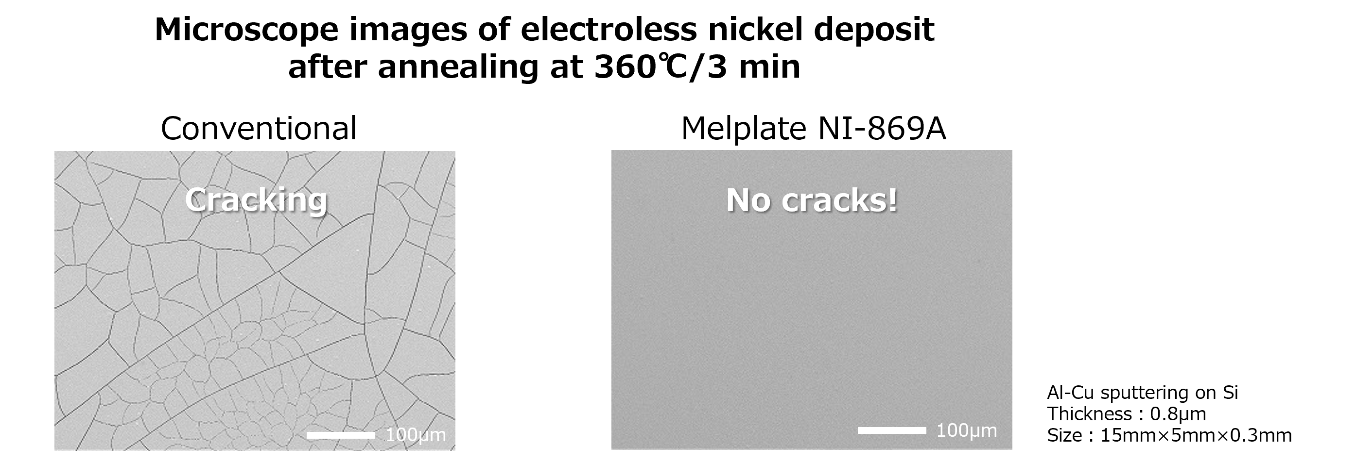
- ・Excellent crack resistance:No cracking after heat treatment at 360°C for 3 minutes
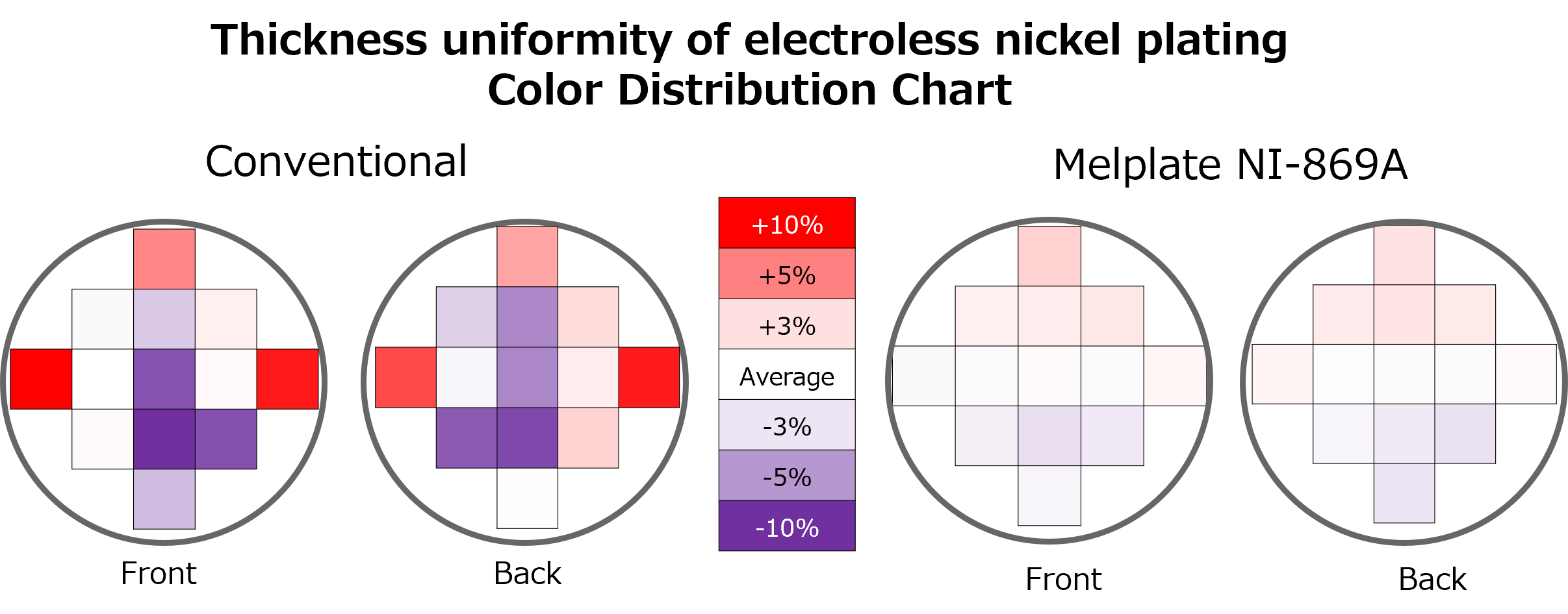
- ・Very small in-plane variation in film thickness.
- ・The amount of nickel film reduction at the solder joint interface is very small.
High heat resistance for high bonding reliability
When heat-treated at 360°C for 3 minutes, electroless nickel-plated films in conventional baths develop cracks, and bonding reliability is not achieved. On the other hand, Melplate NI-869A film shows no cracking even after heat treatment. Conventional electroless nickel plating baths have an amorphous structure immediately after plating, but this structure is subject to structural changes such as recrystallization during heat treatment. However, Melplate NI-869A films show little change in crystal structure due to heat treatment, and cracks are suppressed even after heat treatment.
Achieves high film thickness uniformity
In addition to its high heat resistance, Melplate NI-869A has excellent uniformity of film thickness within the wafer surface. Generally, the deposition rate of electroless nickel is affected by agitation, resulting in variations in film thickness caused by variations in agitation strength. To achieve uniform film thickness, it is important to improve not only the plating solution but also the equipment. Melplate NI-869A minimizes the effect of agitation on plating speed, thereby minimizing the in-plane film thickness due to the properties of the plating solution alone.
Electroless nickel plating bath to ensure bonding reliability
Melplate NI-869A is an electroless nickel plating bath optimized for power semiconductors with high heat resistance and high uniformity of film thickness for UBM formation. Our Melplate UBM process can be used as a pretreatment (→Reference link).The Melplate UBM process can be used to pretreat various Al alloy electrodes for electroless nickel plating with minimal damage.
Contact
Please feel free to contact us regarding more detailed characteristics data, applications, prototyping or any other matters.
We will reply to you by email first.