
Copper sulfate plating bath for via filling application with excellent thickness uniformity
Less sensitive to liquid flows and applicable in the wide range of current densities

Printed Wiring Boards and Plating Technology
Printed wiring boards have been widely used in electronic devices that surround us in our daily lives, such as information terminals including smartphones, sensor modules for an advanced driver-assistance system in automobiles, and data centers that enable information and communication processing that grows in size as IoT technology is implemented. In the manufacturing process of printed wiring boards, various plating technologies are used, including electrolytic copper plating for interlayer connections and circuits formation, electroless copper plating to ensure the conductivity for electroplating, and electroless nickel plating and immersion gold plating for final finish of pads on which electronic components are mounted. In recent years, fine and high-density circuit formation has been required to printed wiring boards in order to meet the demands of high-performance electronic devices, and the performance requirements for copper sulfate plating for interlayer connections and circuits formation have become more diverse and sophisticated.
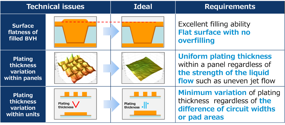
Technical Issues on Copper Sulfate Plating
For multilayer and high-density PWBs, both interlayer connection using blind via holes (BVH) and fine circuit formation through pattern plating are required, and copper sulfate plating technology is facing to the following three challenges.
①Improvement of surface flatness of filled BVH
When filling BVHs with different dimensions, giving the priority to filling ability tends to bring overfilling on BVHs with thin dielectric layers. This is an issue in stacked-via formation.
②Suppression of plating thickness variation within panels
It is difficult to ensure a homogeneous liquid flow to the surface within a panel, and differences in plating thickness within the panel easily occur depending on the strength of the liquid flow.
③Suppression of plating thickness variation within units
Since large-area pads and fine circuit patterns with various line widths are located within an unit, plating thickness difference is easily induced caused by the variation of plating area density.
On copper sulfate plating, uniform plating thickness achievement has been attempted by utilizing the behavior of a leveler component, i.e., copper deposition is suppressed where is exposed to strong liquid flow, for fine pattern formation. On the other hand, uniformity of plating thickness on large pads or within a panel is taken into less account. As a solution to these issues, we have developed a new copper via-filling bath, Lucent Copper IVF, which is less dependent on liquid flow and has excellent deposit thickness uniformity.
Suppression of Overfilling
Lucent Copper IVF is designed to suppress overfilling even when even when surface copper deposit thickness is increased, resulting in achieving flat surface on filled BVHs. This leads to the advantage of facilitating stacked vias in the stacking process of build-up substrates. 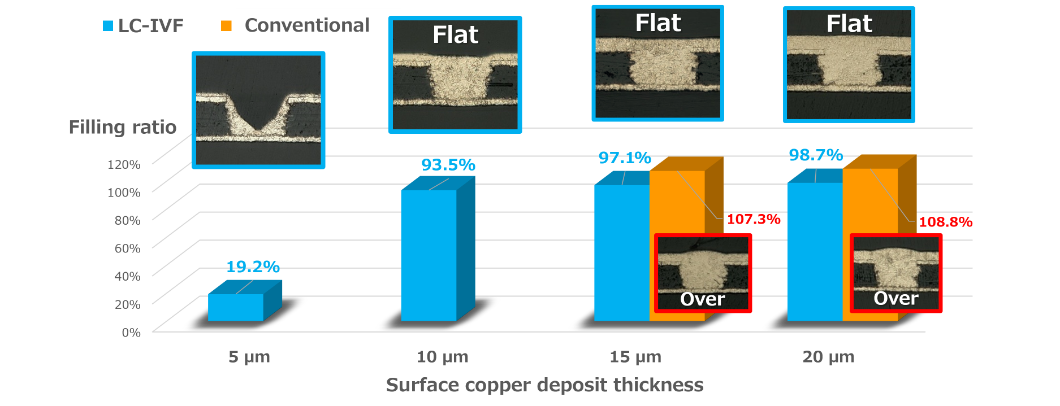

Filling performance independent of liquid flow
Lucent Copper IVF shows excellent filling performance even under a wide range of liquid flow conditions.This liquid flow-independent filling performance reduces differences in via filling performance on various positions within a panel.This feature is also preferable for suppressing the influence of liquid flow difference in different stages of a vertical continuous plating line. 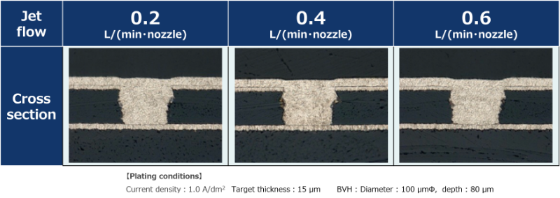
Plating Thickness Uniformity within a Panel
Surface of PWBs is exposed to various liquid flow conditions during plating process. Since Lucent Copper IVF is less sensitive to liquid flow conditions, uniform deposit thickness in a panel is expected. 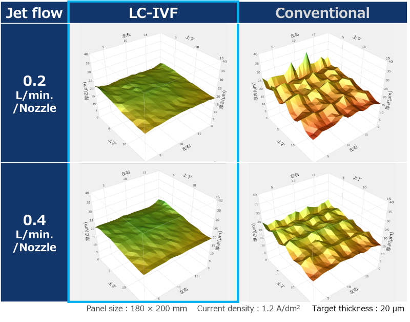
Plating Thickness Uniformity within an unit
Various sizes of pads and widths of circuit patterns are coexisted within an unit on PWBs. Lucent Copper IVF provides uniform thickness performance on these plated surfaces. 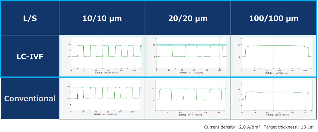
Copper sulfate plating bath with excellent thickness uniformity
Lucent Copper IVF is a copper sulfate plating bath that is less sensitive to the influence of liquid flow in the plating process. Lucent Copper IVF provides reliable filling performance under a wide range of liquid flow conditions and achieves uniform pattern thicknesses. 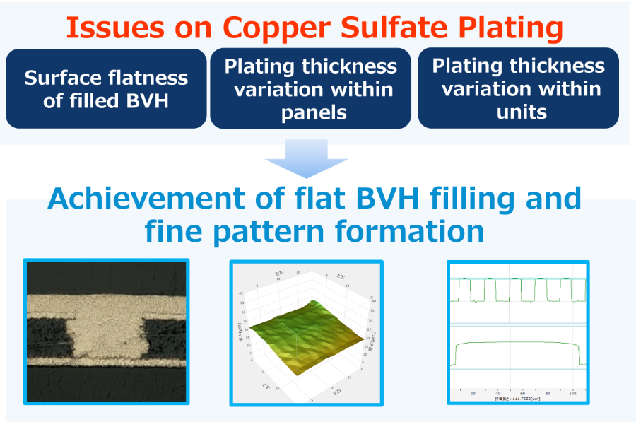
Contact
Please feel free to contact us regarding more detailed characteristics data, applications, prototyping or any other matters.
We will reply to you by email first.