
Copper seed etchant for modified semi-additive process (MSAP)
Melstrip SE-400
Chemicals
PCB
Etching
Copper
Melstrip SE-400
Melstrip SE-400 is an etchant specially desinged to etch copper seed layer on carrier-supported copper foil in modified semi-additive process (MSAP). Undercut or side wall loss of conductuve patterns is effectively suppressed and excellent circuit pattern formation is achieved.
◆Features
1. Flat surface morphology after etching process contibutes to reduction of transmission loss.
2. The stability of the working solution is high compared with a conventional sulfuric acid-hydrogen peroxide type etchant.
◆Features
1. Flat surface morphology after etching process contibutes to reduction of transmission loss.
2. The stability of the working solution is high compared with a conventional sulfuric acid-hydrogen peroxide type etchant.
Surface and cross section of copper patterns after seed layer etching
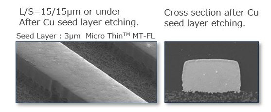
Reduction of transmission loss is the key technology for the next-generation communication standard like 5G. For this, flat copper conductive surface on flat dielectric substrates is high required. Melstrip SE-400 is preferable to achieve flat copper surface after etching compared with a conventional sulfuric acid-hydrogen peroxide type copper etchant.
Cross section of embedded copper patterns
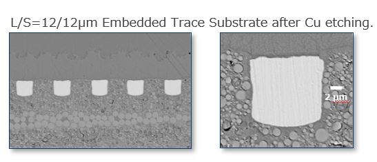
In Embedded Trace Substrates (ETS), the gaps between conductive pattern and resin is protected from permeation of an etchant. The top of conductive patterns, the only part exposed to an etchant in ETS process, maintains its flat and smooth morphology by using Melstrip SE-400. This ensures the flattness of conductive pattern surface, suitable to low transmission loss required for the next-generation communication standard.